jumpincactus
Premium Member
Supporter
- 11,609
- 438
LED tech is predicted to hit 4.19 bil by 2019 with good reason as more and more mfgr's are marketing to both small and large scale growers especially in the burgeoning cannabis market.
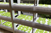
I can remember as the LED craze hit cannabis growers with the marketing promises of less heat and better yields that legacy HID lighting is slowly becoming a thing of the past. However we/they still have a way to go yet to truly bring out the full potential of this exciting tech. One of the remaining challenges is thermal management. Heat and LED's do not play well together. Here is a great article on some of the facts concerning LED's and the heat they produce and what needs to be done to manage the thermal load so the alleged touted 40,000 hr life span of the bulbs can be realized.
With innovations in LED grow lighting, society is on the cusp of a revolution in horticultural production. But, says John Cafferkey, marketing manager of Cambridge Nanotherm, the success of this revolution may hinge on finding ways to improve the thermal efficiency of LED modules…
It’s an incredible time for those in the horticultural industry right now. Arguably, few people outside of the industry realise what a fundamental transformation is currently taking place in terms of how our produce is grown, and some of the far-reaching implications this could have.
For many years high-intensity discharge (HID) lighting has been used as a substitute to natural sunlight. Where it is economical to run them – a critical factor – HID light sources have allowed farmers to grow crops indoors in a controlled environment and to a more flexible schedule (out of season and often year-round).
While HIDs have been the mainstay of many horticulturalists, they are now rapidly being replaced by LED technology. A recent report from RnR Market Research suggests that the LED grow light industry will be worth a whopping $4.19bn by 2022, with a CAGR of 9.63 per cent between 2016 and 2022.
Compared to HIDs, LEDs turn on and off quickly, making them simpler to fit into automated grow cycles. They can also be developed to emit very specific wavelengths of light so they can be ‘tuned’ for different types of crop and for different stages in a plant’s growth cycle.
However, most significantly, LEDs are considerably more cost-effective and cooler running than HIDs. It is these last two properties that reveal the true potential of LED grow lighting.
First, the massively reduced running cost of LEDs opens grow lighting up to a much wider range of crops, including many of those that would have previously been regarded as uneconomical because of their lighting requirements or cheap sale price. In other words, LED grow lighting is making the transition from price-premium produce (for example cannabis) to everyday agriculture.
Secondly, cool-running devices mean that farmers can grow crops in much tighter formations without the danger of heat damage to the plants. This enables some exciting applications, for example in areas such as vertical farming, where produce is stacked tightly in vertical formation, and can be grown close to source, with all of the economies this entails.
Waste heat is still an issue for LED designs
However, while LEDs run much cooler than HIDs, around 60 per cent of the power that goes into them is still outputted as waste heat. This waste heat can pose a serious threat to the lifespan of LEDs.
LEDs are covered by an encapsulant lens to protect them from the atmosphere and diffuse the light they generate. Unfortunately, this lens is also thermally insulating. Thus, the heat generated by LEDs cannot escape via radiation, as it would with a HID lamp. Instead heat must be conducted through the bottom of the LED design.
Should heat fail to be conducted away from the LED effectively the lifetime of the LEDs will be reduced, often catastrophically. LEDs that fail don’t just incur a replacement cost, there’s also the additional maintenance costs involved in constantly replacing them.
What’s more, removing this heat from LEDs is becoming a more pressing problem. For reasons of economy designers are looking to cram more higher powered LEDs (1-5W) into smaller spaces as a means of reducing the materials-cost of their designs. Individual LEDs running at a higher power density in this way present a greater challenge for thermal management systems.
To understand how thermal management can continue to be improved, we need to look at how LED modules are constructed to be thermally efficient.
Fundamental elements of a thermally-efficient LED design
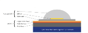
Let’s assume that our example design uses ‘packaged’ LEDs. These are individual LED die that are ‘packaged’ on a thermally-efficient submount with their own encapsulant (so that the whole ‘LED package’ can later be easily mounted onto a PCB). Generally, the submount used underneath the die will be a ceramic. While expensive, ceramics act as an excellent transporter of heat (and heat spreader). This is referred to as ‘Level 1’ (L1) packaging.
The next stage of heat transport must be handled at the board level, ‘Level 2’ (L2). Standard PCBs cannot cope with the thermal demands of horticultural lighting, as the fibreglass/epoxy composites of which they are made is a poor thermal conductor. For this reason, ‘metal clad’ PCBs (MCPCBs) are typically used for such High Power LED designs.
How is an MCPCB constructed? There are a few structural elements that remain broadly similar across all MCPCBs. First you have a copper circuit layer, then a dielectric layer which separates the circuit above from the metal beneath, preventing the two from shorting each other out. Lastly, you have the metal board itself, usually aluminium, but sometimes copper, which transports heat effectively to the system-level assembly (such as a heat sink).
Dielectrics pose a challenge for effective thermal management in MCPCBs
As you’d expect, the copper circuit and aluminium board layers in MCPCBs are both excellent thermal conductors. The same cannot be said for dielectric layers. As the industry has discovered, finding a material that is electrically insulating (up to a suitable breakdown voltage) yet has high thermal conductivity is a real challenge.
The most commonly used approach has been to create a dielectric with a layer of epoxy resin adulterated with thermally conductive ceramic grains to increase the overall thermal conductivity. However, only so much ceramic can be added before the epoxy becomes brittle and starts to crack. And even the best such material on the market can no longer match the thermal demands of horticultural lighting systems.
To enable the continued evolution of horticultural lighting applications many designers today require boards with a level of thermal conductivity higher than ceramic filled epoxy can provide. It’s clear that a new approach is needed.
Nanoceramics: A new way of enabling effective thermal management in MCPCBs
A Cambridge-based nanotech company has developed a new way of addressing this ‘dielectric problem’, with an entirely unique approach to constructing thermally efficient dielectrics.
The company uses a patented electro-chemical oxidation (ECO) process to transform the aluminium surface of a MCPCB into an extremely thin layer (between 10–30µm) of alumina (Al2O3).
Whilst alumina isn’t technically the best material in terms of thermal efficiency, the extraordinary thinness of this dielectric layer renders this fact moot. As heat only has to travel through a few microns of material the overall thermal performance of the stack (the circuit, nanoceramic dielectric and the aluminium board) comes in at 115W/mK – head and shoulders above what can be achieved using alternative approaches.
Ultimately, horticultural lighting designers want their products to be cooler, smaller, brighter and more cost effective. They also want to ensure that they last for their stated lifetime. All of these factors are critical to the continued development of the horticultural lighting sector, and the new wave of farming techniques they enable. And as this market continues to blossom you can expect to see nanoceramics at the core of horticultural LED designs.
www.camnano.com
I can remember as the LED craze hit cannabis growers with the marketing promises of less heat and better yields that legacy HID lighting is slowly becoming a thing of the past. However we/they still have a way to go yet to truly bring out the full potential of this exciting tech. One of the remaining challenges is thermal management. Heat and LED's do not play well together. Here is a great article on some of the facts concerning LED's and the heat they produce and what needs to be done to manage the thermal load so the alleged touted 40,000 hr life span of the bulbs can be realized.
With innovations in LED grow lighting, society is on the cusp of a revolution in horticultural production. But, says John Cafferkey, marketing manager of Cambridge Nanotherm, the success of this revolution may hinge on finding ways to improve the thermal efficiency of LED modules…
It’s an incredible time for those in the horticultural industry right now. Arguably, few people outside of the industry realise what a fundamental transformation is currently taking place in terms of how our produce is grown, and some of the far-reaching implications this could have.
For many years high-intensity discharge (HID) lighting has been used as a substitute to natural sunlight. Where it is economical to run them – a critical factor – HID light sources have allowed farmers to grow crops indoors in a controlled environment and to a more flexible schedule (out of season and often year-round).
While HIDs have been the mainstay of many horticulturalists, they are now rapidly being replaced by LED technology. A recent report from RnR Market Research suggests that the LED grow light industry will be worth a whopping $4.19bn by 2022, with a CAGR of 9.63 per cent between 2016 and 2022.
Compared to HIDs, LEDs turn on and off quickly, making them simpler to fit into automated grow cycles. They can also be developed to emit very specific wavelengths of light so they can be ‘tuned’ for different types of crop and for different stages in a plant’s growth cycle.
However, most significantly, LEDs are considerably more cost-effective and cooler running than HIDs. It is these last two properties that reveal the true potential of LED grow lighting.
First, the massively reduced running cost of LEDs opens grow lighting up to a much wider range of crops, including many of those that would have previously been regarded as uneconomical because of their lighting requirements or cheap sale price. In other words, LED grow lighting is making the transition from price-premium produce (for example cannabis) to everyday agriculture.
Secondly, cool-running devices mean that farmers can grow crops in much tighter formations without the danger of heat damage to the plants. This enables some exciting applications, for example in areas such as vertical farming, where produce is stacked tightly in vertical formation, and can be grown close to source, with all of the economies this entails.
Waste heat is still an issue for LED designs
However, while LEDs run much cooler than HIDs, around 60 per cent of the power that goes into them is still outputted as waste heat. This waste heat can pose a serious threat to the lifespan of LEDs.
LEDs are covered by an encapsulant lens to protect them from the atmosphere and diffuse the light they generate. Unfortunately, this lens is also thermally insulating. Thus, the heat generated by LEDs cannot escape via radiation, as it would with a HID lamp. Instead heat must be conducted through the bottom of the LED design.
Should heat fail to be conducted away from the LED effectively the lifetime of the LEDs will be reduced, often catastrophically. LEDs that fail don’t just incur a replacement cost, there’s also the additional maintenance costs involved in constantly replacing them.
What’s more, removing this heat from LEDs is becoming a more pressing problem. For reasons of economy designers are looking to cram more higher powered LEDs (1-5W) into smaller spaces as a means of reducing the materials-cost of their designs. Individual LEDs running at a higher power density in this way present a greater challenge for thermal management systems.
To understand how thermal management can continue to be improved, we need to look at how LED modules are constructed to be thermally efficient.
Fundamental elements of a thermally-efficient LED design
Let’s assume that our example design uses ‘packaged’ LEDs. These are individual LED die that are ‘packaged’ on a thermally-efficient submount with their own encapsulant (so that the whole ‘LED package’ can later be easily mounted onto a PCB). Generally, the submount used underneath the die will be a ceramic. While expensive, ceramics act as an excellent transporter of heat (and heat spreader). This is referred to as ‘Level 1’ (L1) packaging.
The next stage of heat transport must be handled at the board level, ‘Level 2’ (L2). Standard PCBs cannot cope with the thermal demands of horticultural lighting, as the fibreglass/epoxy composites of which they are made is a poor thermal conductor. For this reason, ‘metal clad’ PCBs (MCPCBs) are typically used for such High Power LED designs.
How is an MCPCB constructed? There are a few structural elements that remain broadly similar across all MCPCBs. First you have a copper circuit layer, then a dielectric layer which separates the circuit above from the metal beneath, preventing the two from shorting each other out. Lastly, you have the metal board itself, usually aluminium, but sometimes copper, which transports heat effectively to the system-level assembly (such as a heat sink).
Dielectrics pose a challenge for effective thermal management in MCPCBs
As you’d expect, the copper circuit and aluminium board layers in MCPCBs are both excellent thermal conductors. The same cannot be said for dielectric layers. As the industry has discovered, finding a material that is electrically insulating (up to a suitable breakdown voltage) yet has high thermal conductivity is a real challenge.
The most commonly used approach has been to create a dielectric with a layer of epoxy resin adulterated with thermally conductive ceramic grains to increase the overall thermal conductivity. However, only so much ceramic can be added before the epoxy becomes brittle and starts to crack. And even the best such material on the market can no longer match the thermal demands of horticultural lighting systems.
To enable the continued evolution of horticultural lighting applications many designers today require boards with a level of thermal conductivity higher than ceramic filled epoxy can provide. It’s clear that a new approach is needed.
Nanoceramics: A new way of enabling effective thermal management in MCPCBs
A Cambridge-based nanotech company has developed a new way of addressing this ‘dielectric problem’, with an entirely unique approach to constructing thermally efficient dielectrics.
The company uses a patented electro-chemical oxidation (ECO) process to transform the aluminium surface of a MCPCB into an extremely thin layer (between 10–30µm) of alumina (Al2O3).
Whilst alumina isn’t technically the best material in terms of thermal efficiency, the extraordinary thinness of this dielectric layer renders this fact moot. As heat only has to travel through a few microns of material the overall thermal performance of the stack (the circuit, nanoceramic dielectric and the aluminium board) comes in at 115W/mK – head and shoulders above what can be achieved using alternative approaches.
Ultimately, horticultural lighting designers want their products to be cooler, smaller, brighter and more cost effective. They also want to ensure that they last for their stated lifetime. All of these factors are critical to the continued development of the horticultural lighting sector, and the new wave of farming techniques they enable. And as this market continues to blossom you can expect to see nanoceramics at the core of horticultural LED designs.
www.camnano.com